Back to Electronics and Semiconductor
Global Thin Wafer Processing and Dicing Equipment Market
Published Date : March 9, 2026 Category: Electronics and Semiconductor
Published Date : March 9, 2026 Category: Electronics and Semiconductor
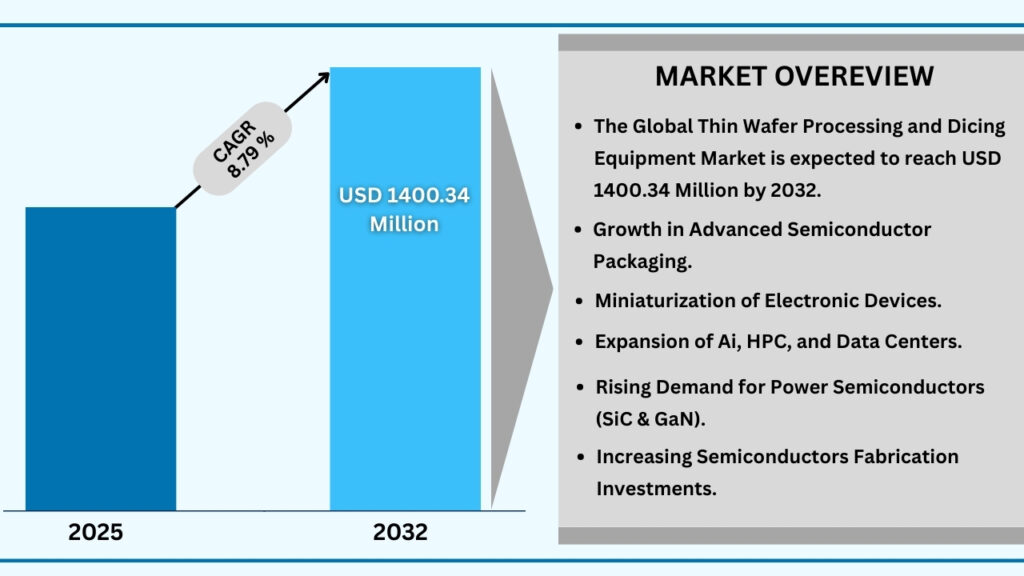
The Global Thin Wafer Processing and Dicing Equipment Market is experiencing significant growth as semiconductor manufacturers push the boundaries of miniaturization, performance efficiency, and advanced packaging technologies. As consumer electronics, automotive electronics, 5G infrastructure, artificial intelligence (AI), and IoT devices demand smaller, faster, and more power-efficient chips, the need for ultra-thin wafers and precision dicing solutions is accelerating.
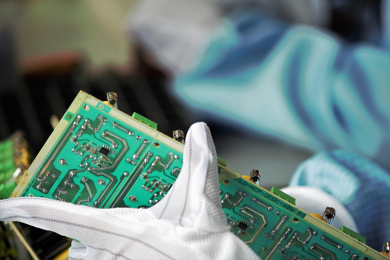
Thin wafer processing involves reducing the thickness of semiconductor wafers to enable advanced packaging architectures such as 3D ICs, fan-out wafer-level packaging (FOWLP), and system-in-package (SiP). Dicing equipment is then used to precisely cut processed wafers into individual chips (dies) with minimal damage and maximum yield. These processes are critical in high-performance computing, memory devices, power semiconductors, and advanced sensors.
As chipmakers move toward heterogeneous integration and chiplet-based architectures, thin wafer technologies are becoming foundational to next-generation semiconductor manufacturing
Market Definition
The Global Thin Wafer Processing and Dicing Equipment Market refers to the industry focused on the development, manufacturing, and deployment of equipment used for wafer thinning, back grinding, polishing, stress relief, and precision dicing in semiconductor fabrication.
Thin wafer processing includes multiple stages such as:
Dicing equipment includes:
These systems are used in semiconductor fabrication plants (fabs), outsourced semiconductor assembly and test (OSAT) facilities, and advanced packaging units. The market supports industries such as consumer electronics, automotive, telecommunications, industrial automation, and aerospace & defense.
Thin wafer processing plays a critical role in enabling compact device design, enhanced thermal performance, and higher electrical efficiency, making it central to advanced semiconductor manufacturing and Industry 4.0 applications.
Industry Scope Explained
The Thin Wafer Processing and Dicing Equipment Market encompasses a comprehensive ecosystem of hardware, software, consumables, and support services that enable precise wafer thinning and die separation in semiconductor manufacturing. The hardware segment includes backgrinders, polishers, bonding/debonding systems, blade and laser dicing machines, and advanced wafer handling tools. Software solutions support process control, yield optimization, defect inspection, and integration with fab automation systems. Consumables such as dicing blades, grinding wheels, tapes, and polishing materials are essential for maintaining performance and precision. Additionally, services including installation, calibration, maintenance, process optimization, and technical support play a critical role in ensuring operational efficiency and long-term equipment reliability.
Hardware Segment
This segment includes advanced backgrinders, chemical mechanical polishers, precision dicing saws, laser and plasma dicing systems, bonding and debonding equipment, as well as automated wafer handling solutions designed for ultra-thin substrates. These systems are engineered to operate with extreme accuracy and stability, where precision alignment, vibration control, temperature regulation, and contamination-free processing are critical performance parameters. Given the fragility of thin wafers, maintaining mechanical stability and cleanroom integrity is essential to prevent cracking, warping, particle contamination, and yield loss during high-volume semiconductor manufacturing.
Software and Automation
Advanced thin wafer processing and dicing equipment increasingly integrates AI-driven process control, real-time defect inspection, yield monitoring analytics, and predictive maintenance software to enhance precision and operational efficiency. These intelligent systems continuously analyze process parameters, detect anomalies, and optimize performance to minimize wafer breakage and improve throughput. Seamless integration with fab automation platforms and Manufacturing Execution Systems (MES) ensures end-to-end process visibility, accurate data tracking, and synchronized production workflows, enabling semiconductor manufacturers to maintain high yield levels and consistent quality standards across high-volume operations.
Services and Support
Installation, calibration, process optimization, maintenance contracts, spare parts supply, and technical consulting represent a significant revenue stream within the thin wafer processing and dicing equipment market. As wafer thickness levels drop below 50 microns, substrates become increasingly fragile and sensitive to mechanical stress, thermal variation, and contamination. This makes ongoing technical support, periodic system tuning, and expert process management essential to maintain yield, minimize breakage, and ensure stable, high-precision operations in advanced semiconductor manufacturing environments.
Thin wafer technologies are widely deployed in:
The growing shift toward chiplet architectures and high-density packaging is expanding the application scope of thin wafer equipment.
Key Advantages of Thin Wafer Processing and Dicing Systems
Enhanced Device Miniaturization
Thinner wafers enable compact device assembly and high-density stacking in 3D packaging structures. This is essential for smartphones, wearables, and portable electronics where space optimization is critical.
Improved Thermal and Electrical Performance
Reduced wafer thickness enhances heat dissipation and electrical efficiency. This is particularly important for high-performance computing and automotive power devices where thermal management is crucial.
Higher Yield and Precision
Modern dicing systems—especially laser and plasma dicing—minimize mechanical stress and chipping. This reduces die damage and increases production yield, directly improving profitability.
Support for Advanced Packaging Technologies
Thin wafer processing is indispensable for technologies such as:
These packaging innovations are central to next-generation semiconductor design.
Market Barriers and Industry Constraints
High Capital Expenditure
Thin wafer processing and precision dicing equipment require substantial capital investment. Advanced laser and plasma dicing systems are particularly expensive, limiting adoption among smaller fabs and OSAT players.
Process Complexity and Yield Risks
Ultra-thin wafers are fragile and prone to warping, cracking, or breakage. Maintaining yield at reduced thickness levels requires sophisticated handling systems and tight process control.
Supply Chain Sensitivity
The semiconductor equipment industry is sensitive to cyclical demand patterns. Capital expenditure fluctuations by major foundries and integrated device manufacturers (IDMs) can impact equipment orders
Regional Dynamics: North America, Europe, and Asia-Pacific
Asia-Pacific
Asia-Pacific dominates the market, driven by strong semiconductor manufacturing presence in Taiwan, South Korea, China, and Japan. Leading foundries and OSAT providers in the region are heavily investing in advanced packaging and wafer thinning technologies to meet global chip demand.
North America
North America plays a strategic role due to its advanced semiconductor R&D ecosystem and leading integrated device manufacturers. Investments in domestic semiconductor production and advanced packaging capabilities are strengthening demand for thin wafer equipment.
Europe
Europe’s market growth is supported by automotive semiconductor manufacturing, power electronics innovation, and strong industrial automation demand. The region is increasingly investing in SiC and GaN-based power devices, which require specialized wafer processing solutions.
Competitive Environment and Key Participants
The market is technology-intensive and characterized by strong R&D investment and high entry barriers. Companies compete on precision, automation capabilities, throughput, yield optimization, and integration flexibility.
Key participants include:
These companies are investing in next-generation laser dicing, AI-based defect detection, ultra-thin wafer handling systems, and environmentally efficient processing technologies.
Strategic partnerships with foundries and OSAT companies are common, ensuring customized solutions aligned with evolving packaging architectures.
Future Market Direction
The future of the thin wafer processing and dicing equipment market lies in greater precision, automation, and sustainability.
AI-enabled process optimization will improve yield at ultra-thin levels.
Increased adoption of laser and plasma dicing will reduce mechanical stress and improve edge quality.
Growth in electric vehicles and renewable energy will drive demand for power semiconductor wafer processing.
Advanced packaging trends such as chiplet integration and 3D stacking will further increase reliance on thin wafer technologies.
Sustainability considerations are also becoming important. Equipment manufacturers are developing energy-efficient systems and reducing water and consumable usage in back grinding and polishing processes.
Conclusion
The Global Thin Wafer Processing and Dicing Equipment Market is a critical enabler of advanced semiconductor manufacturing. As devices become smaller, faster, and more complex, ultra-thin wafer processing and precision dicing technologies are becoming indispensable.
While high capital investment and process complexity remain challenges, continuous innovation and expanding application areas are driving long-term growth. Companies that invest in high-precision, scalable, and AI-enabled wafer processing solutions will be best positioned to capture opportunities in the evolving semiconductor landscape.
In the era of advanced packaging, chiplet integration, and high-performance electronics, thin wafer processing is not just a manufacturing step—it is a strategic pillar of semiconductor innovation.
At Advantia Business Consulting, we help semiconductor equipment manufacturers, technology providers, and investors navigate rapidly evolving markets such as thin wafer processing and precision dicing technologies. Through comprehensive market intelligence, strategic advisory, and competitive landscape analysis, we enable clients to identify emerging opportunities in advanced packaging, power semiconductor manufacturing, and next-generation chip architectures. With deep insights into global semiconductor trends, Advantia Business Consulting supports organizations in making informed decisions and building resilient strategies in the high-growth semiconductor ecosystem.